Warranties For Quick Turn PCBs
The ability to get electronic products to market quickly depends on the rapid manufacturing capabilities of PCBs. This type of fabrication is critical in the prototype, pre-production and full production phases. A quick turn PCB manufacturer should have adequate capacity, equipment and processes to deliver high quality results with consistent timelines.
Typical turnaround times are tabulated in most quick turn pcb boards supplier websites to guide customers with their decision making. However, to ensure that the project is completed on time it is important that all the requirements are clearly defined at the beginning of the process. Any potential issues should have a detailed mitigation plan so they can be corrected as early as possible.
In most cases, quick turn fabrication is a good option for prototyping as it allows errors to be detected and fixed early in the process. This reduces the costs of expensive fixes during a high-volume run and ensures that the final product will be functional when it is released to market.
Typical Warranties For Quick Turn PCBs
To ensure that a quick turn PCB is made correctly, the design must be submitted in a format that the fab shop can accept. This file type is called Gerber files and dictates to the equipment what the layers should look like. In addition, an aperture library and drill file must be submitted to tell the fab what holes to use for the components.
Once the files are received, the fab shop begins to build the boards. This stage can take a while depending on the complexity of the board and the number of layers. When the bare boards are fabricated, they must undergo visual inspection and electrical testing to check for circuit defects like shorts and opens. This can be done manually using flying probe testers or with automated optical inspection systems like AOI.
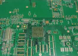
For PCBs with multi-layers, it is important to ensure that the copper traces and land fills are not too close to the edges of the board as this can lead to problems during assembly and soldering. This can also cause issues with the connection between the layers in the resulting PCB. To ensure the best outcome, it is essential that all layers are separated by at least 0.010″ (0.1 mm) to prevent traces from being exposed.
The choice of materials for the bare boards can impact the turnaround time as well. The fabricator should have enough stock to meet most needs, but special or exotic materials may need a few weeks to be purchased and processed. In this case, the engineer should plan ahead and make sure the fabrication schedule takes these delays into account. It is also a good idea to have a backup material source for any emergencies that might arise. This can save the customer significant delay and cost when there are supply chain issues beyond their control.