Evolution and Impact of HDI PCB Technology
In the ever-evolving landscape of electronics manufacturing, High-Density Interconnect (HDI) printed circuit boards (PCBs) have emerged as a cornerstone technology, enabling the development of smaller, more powerful, and sophisticated electronic devices. HDI PCBs represent a significant advancement over traditional PCBs, offering enhanced performance, increased functionality, and greater design flexibility. This article delves into the evolution, features, and impact of HDI PCB technology on the electronics industry.
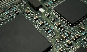
HDI PCBs have revolutionized the way electronic devices are designed and manufactured. Unlike conventional PCBs, which feature a single or double layer of copper traces, HDI PCBs integrate multiple layers of intricate circuitry within a compact space. This is achieved through the use of advanced manufacturing judi resmi techniques such as microvia drilling, sequential lamination, and laser drilling, which allow for the creation of extremely fine traces and vias with high-density interconnections.
One of the key advantages of hdi pcb is their ability to accommodate the ever-shrinking form factors of modern electronic devices. As consumer demand for smaller, lighter, and more portable gadgets continues to rise, manufacturers are under pressure to pack more functionality into limited space. HDI PCBs address this challenge by offering higher routing densities, finer lines and spaces, and increased layer counts compared to traditional PCBs. This allows designers to optimize board real estate and maximize component placement efficiency, resulting in more compact and feature-rich electronic products.
Exploring the Evolution and Impact of HDI PCB Technology
Moreover, HDI PCBs deliver superior electrical performance and signal integrity, thanks to their reduced parasitic capacitance and impedance. By minimizing signal degradation and interference, HDI technology enables high-speed data transmission, low-power consumption, and reliable operation in demanding applications such as telecommunications, aerospace, and medical devices. This makes HDI PCBs the preferred choice for mission-critical systems where performance and reliability are paramount.
Another compelling feature of HDI PCBs is their enhanced thermal management capabilities. As electronic devices become more powerful and densely packed, managing heat dissipation becomes increasingly challenging. HDI technology addresses this issue by incorporating advanced thermal vias and conductive materials that efficiently channel heat away from critical components, thereby preventing overheating and ensuring long-term reliability. This is particularly important in high-power applications slot server thailand super gacor such as automotive electronics and industrial control systems, where thermal management is a critical design consideration.
Furthermore, HDI PCBs offer greater design flexibility and manufacturing efficiency compared to traditional PCBs. The use of advanced CAD/CAM software and automated assembly equipment enables designers to create complex layouts with unprecedented precision and speed. This streamlines the prototyping and production process, reduces time-to-market, and lowers overall manufacturing costs. Additionally, HDI technology supports the integration of advanced features such as blind and buried vias, controlled impedance, and fine-pitch components, further expanding the design possibilities for electronic engineers.
In conclusion, HDI PCB technology represents a significant in the evolution of electronic manufacturing, offering unparalleled performance, functionality, and design flexibility. As the demand for smaller, more powerful electronic devices continues to grow, HDI PCBs will play an increasingly integral role in shaping the future of technology. By enabling the development of innovative products with enhanced capabilities and reliability, HDI technology is driving progress and innovation across a wide range of industries, paving the way for the next generation of electronic devices.